Most people (well, let’s assume most people love physical science, especially light matter interaction) have a rough understanding about photonic crystals (PCs). To start with -- photonic crystals (PCs) are periodic optical nanostructures that are designed to manipulate light. In general, to affect light’s propagation, the length of the repeating unit cell of the nanostructures in PCs is compatible to the wavelength of light. If you reach this far, you know quite a lot about PCs.
The next thing in our mind would be “where are the examples”!? If you follow scientific news closely, you might say – “Invisible cloak is made by PCs according to a BBC report or an article on sceince.” This is definitely true. However, there are a lot more applications based on PCs that are exciting and deserve us to take a detailed look. Furthermore, these applications are close to real world applications than you think!
Let us start with two-dimensional(2D) PCs. 2D PCs mean the unit cell is extending in two dimensions, just like the silicon slab shown in figure 1. In this case, we can picture the unit cell of the nanostructure is the air hole which extends in a plane. The light will be launched into the waveguide in the middle of the slab. Pioneered by Professor Susumu Noda (plenary speaker of CLEO 2011), this kind of silicon slab is a “light master”. By fine-tuning the air hole patterns, sizes and the positions, light with different frequencies will choose completely different routes when propagating in the waveguide through the slab. In general, the air hole size decides which frequency can leave the waveguide while the missing air holes (point defect) in the nanostructure determines where the light would be located and emitted. For example, the slab shown in figure 2 is an amazing design. It is a slab composed of seven PCs with different air hole sizes. In each PC, there is a point defect where three air holes are missing. Light with different frequencies chooses to leave the main highway (waveguide) and emits at different locations (point defect) as shown on the left of figure 2. The air hole has the size of about 400nm and the difference in air hole diameter of PC1 and PC7 is just 7 nm! These small structures and the differences in structures have huge effect on the light propagating.

 |
Figure 1. A silicon 2D PC. |
 |
Figure 2. A seven-component 2D PC. Each PC is capable of selecting one frequency and emits it into the space. A mini-optical circuit indeed. Courtesy and copyright of B. Song, S, Noda, and T. Asano, Science 300 1537 (2003). |
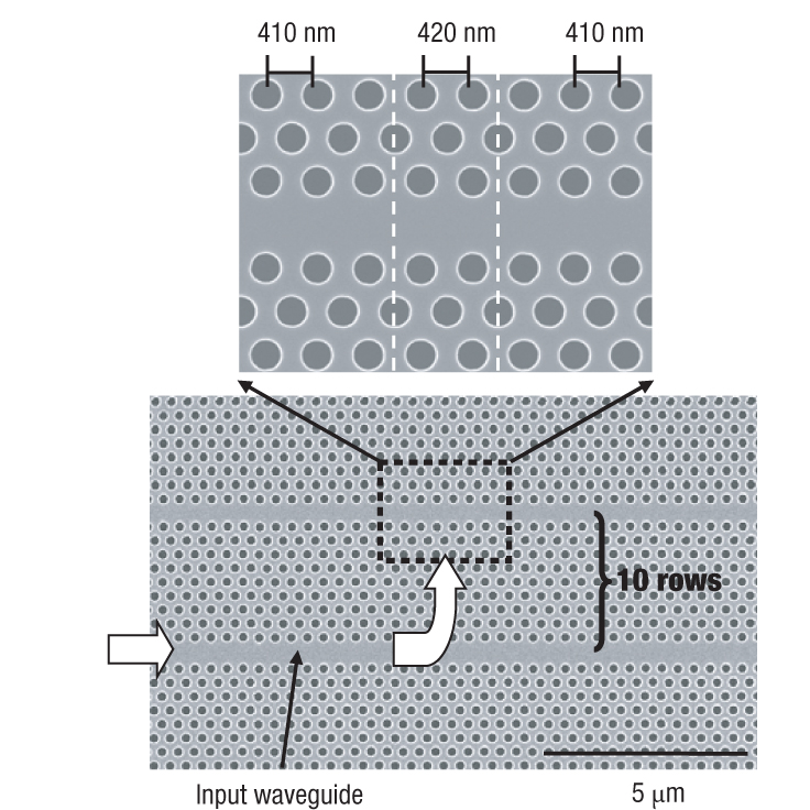
In addition to using the “point defect”, changing the hole sizes proves to be another neat way to localize the light, As shown in figure 3 (upper panel), the upper part of the slab is composed of air holes of diameter 410nm and 420nm, respectively. The difference is so small such that you can not tell easily even by a TEM image. If we launch the light through the lower waveguide, and scan the frequency of the laser, we found there is only one frequency that will hop into upper waveguide and be localized in a nanoscale volume (figure 3, lower panel). Furthermore, this method can select a very narrow bandwidth compared with the “point defect” method. As a result, it proves to have a much higher Q-factor in the localized cavity.
 |
Figure 3. A highly selective 2D PC based on different air hole sizes. The inset on the lower panel shows the near field image of the dashed rectangle. Courtesy and copyright of B. Song, S. Noda, T. Asano, and Y. Akahane, Nature Materials 4 207 (2005). |
Same idea can be applied to three dimensions. An interesting example is to suppress the spontaneous emission (SE) of a device (quantum well, for example). Modern techniques allow us to create a 3D PC such that certain frequencies of light cannot propagate in it. The set of the frequencies that are forbidden to propagate is called photonic bandgap (PBG). Now, if we embed a device into a 3D PC where the SE has the frequency in the PBG of this 3D PC, interesting things will happen. Since none of the accepting mode of the SE can exist or propagate in all directions, the emission lifetime is found to increase by several folds. Considering SE is not desirable in a laser system since it sets the threshold for the laser when it tries to lase and we cannot harvest the energy that is produced by SE in most cases, controlling the SE is indeed a great achievement.
Another nanostructure that is fascinating is a low dispersion optical fiber that can transport femtosecond light without adding too much dispersion. Creating a near chaos and/or random nanostructure such that no light frequency is resonant or interact constructively to it except propagating through the guided mode is the key. One example is shown in figure 4. An experiment shows that a 13 fs pulse only stretches to 26 fs when propagates in this fiber for a distance of 1 meter. This is a substantial improvement if we consider that normally a meter of fiber would stretch the pulse into ps regime. Maybe soon in the near future, we can transport ultra short pulse through fiber without stretching it!
I hope by now you are already fascinated by PCs…^_^.
 |
Figure 4. The fiber core of a low dispersion optical fiber. Notice the structure has no periodicity at all. Courtesy and copyright of J. Bethge, G. Steinmeyer, S. Burger, F. Lederer, R. Iliew, IEEE J. Lightwave Technol. 27, p. 1698 (2008). DISCLAIMER The opinions expressed herein are those of the author and do not represent the Optical Society of America (OSA) or any OSA affiliate. |